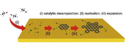
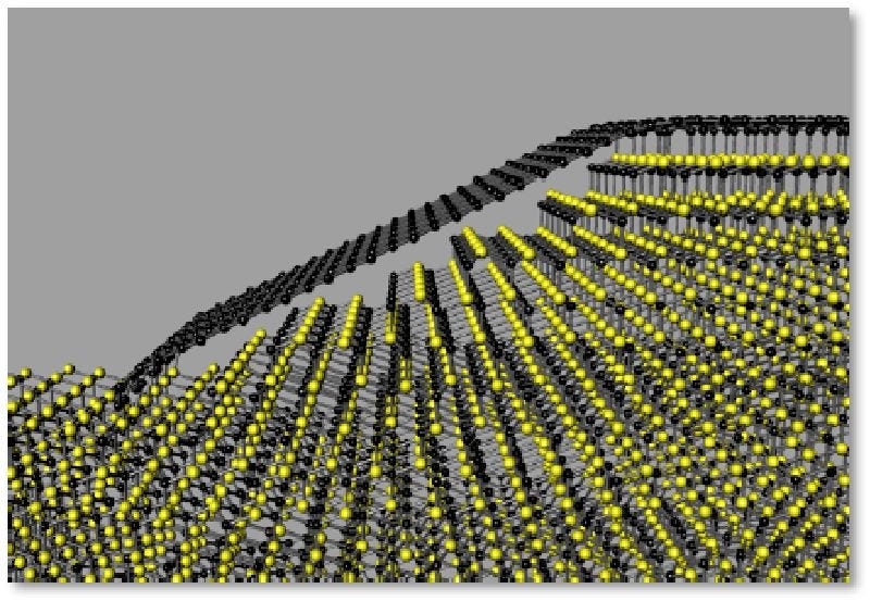
Image Courtesy: Xiangping Chen, Lili Zhang, Shanshan Chen - Xiamen University (China) & Institute of Chemical Engineering and Sciences (Singapore)
Since graphene’s performance is very susceptible to contamination and structural defects (such as folds, grain boundaries, and pin holes) from processing or the transfer process, a review of graphene growth techniques should be done to determine the benefits and drawbacks of each. Due to the sensitivity of graphene, the growth method must be chosen with the required quality, processing, scale, and device architecture in mind, making exfoliation good for small test structures but inadequate for a repeatable semiconductor targeted process.
There are five major pathways for creating graphene sheets: exfoliation from bulk graphite, unzipping through etching a carbon nanotube, growth from sublimation and reconstruction of carbon from a carbide surface, epitaxial growth from a carbide forming catalyst layer by utilizing condensation during cooling, and the epitaxial growth utilizing a non-carbide forming catalyst layer.
Image: Fabrication schemes for the large scale synthesis of graphene sheets
Exfoliation
As of 2014, exfoliation methods produced graphene with the lowest number of defects and the highest electron mobility by the pioneers of graphene, Novoselov and Geim, using the adhesive tape method to isolate graphene from graphite. The most common exfoliation method utilizes an adhesive tape to pull graphene films off a graphite crystal, which are subsequently thinned down by further strips of tape and finally rubbed against the desired substrate. This rather crude method creates a random array of single and double layer graphene flakes on the desired substrate that has been a key driver for investigating the many properties of graphene. Since graphene is susceptible to creating folds during this process, it cannot be produced with high accuracy and repeatability, so other mechanical and chemical exfoliation processes have been investigated. To address the difficulties of the scotch tape method, one group tried to exfoliate graphene from highly ordered pyrolytic graphite (HOPG) utilizing a sharp single-crystal diamond wedge penetrating into the graphite source to exfoliate layers. This method has problems with defect initiation through shear stress and the reliable placement of the graphene flakes after exfoliation.
The other main exfoliation method is to utilize liquid-based techniques to create a dispersion of graphene or graphene oxide flakes that are drop-casted or ink-jet-printed, and in the case of graphene oxide subsequently reduced. Liquid exfoliation can be accomplished through the use of solvents or ionic liquids with similar surface tension to graphene, which when sonicated exfoliate the bulk graphite into graphene sheets that can be subsequently centrifuged to create a supernatant and dispersed. Probably the oldest known method for producing graphene is through the production of graphite oxide using Hummers’ method, sonicating to create a dispersion and then reduction of the graphene oxide either through the introduction of hydrazine at elevated temperature or through the introduction of a quick burst of energy introduced either through a light burst or a temperature spike.
Image: Reduction of graphene oxide using a LightScribe laser writing system ion, a standard DVD writer
Carbon nanotube unzipping
Graphene can be created by cutting open carbon nanotubes. In one such method, multi-walled carbon nanotubes are cut open in a solution by action of potassium permanganate and sulfuric acid. In another method, graphene nanoribbons were produced by plasma etching of nanotubes partly embedded in a polymer film. This method is useful for producing nanoribbons of graphene that induces a band gap in graphene through geometry breaking. However, the placement of the nanotubes on an integratable chip has been problematic, and thus this method once again is only good for the production of test structures to probe graphene characteristics.
Image showing the unzipping of a carbon nanotube to produce graphene sheets
Sublimation and reconstruction from carbide
Heating silicon carbide (SiC) or other carbide materials (TaC, NbCm ZrC, HfC, TiC) to high temperatures (>1,100°C) under low pressures (~10-6 torr) boils off the Si (from either the Si face or underlying Si from the C face) and reconstructs the C into a single layer graphene film, although multi-layer graphene has been produced through this approach as well. This process produces epitaxial graphene with dimensions dependent upon the size of the wafer.
Image: Bonding of graphene at a SiC step Edge
Growth through condensation after carbide formation
Graphene growth utilizing a carbonaceous source material (such as methane introduced through a CVD process) differs from material to material with the carbon solubility in the metal and the growth conditions determining the deposition mechanism. For carbide producing metallic substrates (such as Ni), graphene growth occurs through a precipitation process during cooling from the carbide. The solubility of C in the metal (Ni for example) is higher at higher temperatures, and thus during the furnace cooling phase carbon diffuses out of its Ni host. The process of forming graphene on Ni has the fundamental limitation that single and few layered graphene is obtained over few to tens of micron regions and not homogeneously over the entire substrate. The lack of control over the number of layers is attributed to the difference in out-diffusion of C from the grains and the grain boundaries of Ni creating non-homogeneous growth conditions.
Epitaxial growth of graphene on a non-carbide forming catalyst
Epitaxy refers to the deposition of a crystalline overlayer on a crystalline substrate, where there is registry between the two. In some cases, epitaxial graphene layers are coupled to surfaces weakly enough (by Van der Waals forces) to retain the 2D electronic band structure of isolated graphene. It is commonly accepted that the production of graphene through the surface absorption of carbon on a non-carbide producing metal (such as Cu or Ir) is an epitaxial process due to the registry between the underlying Cu (or Ir) crystal structure and the graphene layer.
Image: Schematic diagram of carbon growth on catalyst forming polycrystalline graphene. With all the challenges discussed, graphene growth by CVD is still a promising process compared with others. Its intrinsic properties stimulate more and more people to involve in the field of CVD graphene
Exceptional high-quality single layer graphene growth over large areas have been recently achieved on polycrystalline copper foils.The growth on Cu or Ir is simple and straightforward due to the metallic substrates not having a stable carbide material, thus the decomposition of C is only reliant upon the grain orientation. For example, Cu is an FCC lattice with three dominant grain orientations Cu(100), Cu(110), and Cu(111) along with high index facets which are made up of combinations of low index facets. Cu(100), Cu(110), and Cu (111) have cubic, rectangular, and hexagonal geometries making the Cu(111) grain orientation able to support epitaxial growth. Thus, grain growth on Cu(111) grains tend to be monolayered graphene sheets while Cu(100) and Cu(110) geometries prevent C diffusion causing compact multilayered C islands to form with higher index facets replicating the performance of the lower index grains.
Don't hesitate to subscribe if you haven't already done so.
Regards and take care.
Born in 2012, Scixel is a project devoted to the improvement of the scientific comunication through the creation of graphical products: pictures, animations, graphs, posters, etc. Scixel consists of scientists with a deep knowledge in digital graphics but also with a long experience in giving talks, preparing posters and papers and other daily situations of scientific work.
We have focused our work into universities and research institutes all over the world: TuDelft (The Netherlands), NIMS (Japan), Basel University (Switzerland), Universidad Autónoma de Madrid, CNB or ICFO (Spain), to name a few.
Web: https://scixel.es/
If you are a company or an individual who would like to place your advertising in my newsletter you can contact me (email) and let me know your request of type of ad and number of newsletters you would like to place it. I will send you a budget as soon as possible.


