GrapheneforUS – Day 1 (Summary)
The GrapheneforUS2021 Online Conference taked place during the 23-24 February.
I would like to present in this post a summary of the first day and invite my readers to read in 7 days of the summary of the second day.
I hope that will be of interest. Currently, the situation in the world does not allow us to travel to organize events and we have to carry out these events online that so far are being kindly accepted by the scientific community.
GrapheneforUS 2021 online was a 2 days event that means to gather the key players of the Graphene Community and related sectors. This event was launched again following the success of the 2018, 2019 & 2020 in-person editions and the lack of meetings in the field in the US. Graphenefor US is now already an established event attracting global participants and sharing, exchanging, exploring new avenues of graphene-related scientific and commercial developments.
The speakers of the first day with their titles were:
Jun Lou (Rice University, USA) - Electrochemical Behaviors of Two-Dimensional Materials for Energy and Environmental Applications
Francesco Bonaccorso (BeDimensional, Italy) - Large-scale production of 2D crystals for energy applications
Richard Kaner (UCLA, USA) - Graphene Synthesis and Applications in Supercapacitors
Gordon Harling (CMC Microsystems, Canada) - Accessing Infrastructure for Prototyping and Measurement
Gordon Rinke (AMO GmbH, Germany) - Wafer Scale Integration of Graphene - 2D Experimental Pilot Line at AMO
Elías Torres Alonso (Graphenea, Spain) - Graphenea Foundry: a platform for the manufacture of graphene-based devices
Niels Wijnaendts van Resandt (Heidelberg Instruments, USA) - Direct Write Lithography Tools and Applications
Mario Lanza (KAUST, Saudi Arabia) - Wafer-scale integration of two-dimensional materials in high-density memristive crossbar arrays for artificial neural networks
An Chen (Semiconductor Research Corporation, USA) - Nanoelectronics Research for Computing beyond CMOS
Mohamed Boukhicha (BNL, USA) - Large-scale Lithium-intercalated Multilayer Graphene Production
Adina Luican-Mayer (University of Ottawa, Canada) - Visualizing 2D materials at the atomic scale
Andrey Krayev (HORIBA Scientific, USA) - Nanoscale Structural Peculiarities in Mono- to Few-Layer Crystals of Ti3C2Tx MXene Revealed by TERS.
Sonia Conesa Boj (TU Delft, The netherlands) - From crafting to visualization: low-dimensional TMD nanostructures under the electron microscope lamppost
Avik Ghosh (University of Virginia, USA) - Unconventional switching using topological properties of electrons in graphene based heterostructures
Bruno Dlubak (CNRS/Thales, France) - Spin filtering in graphene based magnetic tunnel junctions
Aida Ebrahimi (Pennsylvania State University , USA) - All-Ink Dopamine Sensors with Ultralow Detection Limit Enabled by One-Step Annealing of Graphene Ink
Salvatore Polverino (Università degli studi di Genova, Italy) - Few-layer graphene-based sustainable cement mortar
Dmitri Efetov (ICFO, Spain) - Competing phases of correlated Chern insulators in Superconducting Twisted Bilayer Graphene
Emanuel Tutuc (The University of Texas at Austin, USA) - Correlated Insulators and Topological Transport in Twisted Double Bilayer Graphene
Arend Van der Zande (University of Illinois, USA) - Electromechanical systems enabled by interfacial slip in 2D material heterostructures
Abhay Pasupathy (Columbia University, USA) - Quantum phenomena in moire heterostructures
Matthew Yankowitz (University of Washington, USA) - Tunable correlated and topological states in twisted monolayer-bilayer graphene
Fida Ali (Sungkyunkwan University, South Korea) - Density of Interface States in Layered-WSe2 Semiconductor
Tien Dat Ngo (Sungkyunkwan University, South Korea) - Fermi-level de-pinning at the intrinsic WSe2-metal junction via van der Waals bottom contacts
Pawan Srivastava (Sungkyunkwan University, South Korea) - Resonant tunneling through twisted black phosphorus homostructures
I would like to highlight some of the talks on this first day.
Bio: Jun Lou obtained B.E. and M.S. degrees in Materials Science and Engineering from Tsinghua University and Ohio State University, respectively, and his Ph.D. degree from the Department of Mechanical and Aerospace Engineering and Princeton Materials Institute at Princeton University. After a brief postdoc at Brown University he joined Rice University, and directs the Nanomaterials, Nanomechanics and Nanodevices Lab (N3L). He is currently a full professor and the associate chair of the Department of Materials Science and NanoEngineering. Lou was an AFOSR Young Investigator and a recipient of Charles Duncan Award for Outstanding Academic Achievement at Rice. He is the Editor-in-Chief of Materials Today, the Elsevier flagship journal covering original research and reviews in the broader materials science community. He currently serves as the site director for the NSF industry university collaborative research center (IUCRC) of Atomically Thin Multifunctional Coatings (ATOMIC) that has 12 member companies, exploring potential applications of 2D materials in different industries with commercial partners.
Abstract: In this talk, several aspects of the electrochemical behaviors of two-dimensional (2D) materials for energy and environmental applications will be discussed. We developed a local probe electrochemical measurement method and successfully applied it to the electro-catalytic activity measurement of various kinds of transition metal dichalcogenides. The catalytic activity and turnover frequencies of the 2H-MoS2 basal plane versus edge as well as the 1T’-MoS2 basal plane are identified by this measurement. At the same time, the basal plane activity and turnover frequencies of transition metal dichalcogenides from different element groups has been systematically studied. We have shown that the general trend of the transition metal dichalcogenides in the form of volcano plot follows the trend of metals. VB-VIA dichalcogenides have been identified as the preferred selection for non noble metal hydrogen evolution reaction (HER) catalysts. Finally, we will demonstrate the application of 2D h-BN as high-performance anti-corrosion coatings for lectrothermal membrane distillation of hypersaline waters.
Bio: Mario Lanza is an Associate Professor of Materials Science and Engineering at the King Abdullah University of Science and Technology (KAUST), in Saudi Arabia. He has has published over 120 research papers (including Science, Nature Electronics) and registered four patents, one of them granted with 5.6 Million CNY. He has received the 2017 Young Investigator Award from Microelectronic Engineering (Elsevier), the 2015 Young 1000 Talent award, and in 2019 he was appointed as Distinguished Lecturer of the IEEE - Electron Devices Society (EDS). Prof. Lanza is Associate Editor of Scientific Reports (Nature) and Microelectronic Engineering (Elsevier), and he serves in the board Advanced Electronic Materials (Wiley-VCH), Nanotechnology and Nano Futures (IOP). He has served in the technical committees of several world-class international conferences, like IEEE-IEDM.
Abstract: Memristors have attracted enormous interest due to their excellent capability to store digital information, and they are being considered to be a key element to build future artificial neural networks for bio-inspired neuromorphic computing systems. Recent works have shown that memristors made of layered twodimensional (2D) materials can exhibit performances that traditional memristors (made of transition metal oxides) do not show, such as excellent transparency and flexibility, high-temperature stability, and unique controllability of the conductance potentiation, depression and relaxation. However, most studies on 2D materials based memristors focused on single devices, and system level performances like yield and device-todevice variability have never been analyzed in depth, despite the great interest that they have raised In this talk, I will present the first wafer-scale statistical analysis of high-density memristive crossbar arrays made of 2D layered materials, their nanoscale electronic characterization with conductive atomic force microscopy, and their application to neuromorphic computing.
Bio: Prof. Dmitri K. Efetov (M) received a Diploma (M.Sc.) in Physics from ETH Zurich (Switzerland) in 2007, and a M.A., M. Ph. and a Ph.D. in Physics from Columbia University (USA) in 2014, under supervision of one of the pioneers of graphene Prof. Philip Kim. Prior to joining ICFO in 2017, he had worked as a postdoctoral researcher at the Massachusetts Institute of Technology (MIT, USA). Since 2017 Dmitri is a professor and group leader at ICFO, whose research program concentrates on the development of novel composite materials known as “van der Waals (vdW) hetero-structures”, which consist of graphene and other 2D materials. Dmitri received the Charles H. Towns Award for his outstanding research achievements during his PhD, and the Obra Social ”la Caixa” Junior Leader Fellowship and an ERC starting grant to start his independent research group at ICFO. Prof. Efetov is leader of the 2D-SIPC project in the Quantum Flagship (1B€ project for 10 years), as well as a member of its Science and Engineering board
Abstract: Flat-bands in magic angle twisted bilayer graphene (MATBG) have recently emerged as a rich platform to explore strong correlations, superconductivity and magnetism. Here we use magneto-transport and Hall measurements to reveal a rich sequence of wedge-like regions of quantized Hall conductance with Chern numbers C = ±1, ±2, ±3, ±4 which nucleate from integer fillings of the moiré unit cell 𝜈 = ±3, ±2, ±1, 0 correspondingly. We interpret these phases as spin and valley polarized many-body Chern insulators. The exact sequence and correspondence of Chern numbers and filling factors suggest that these states are driven directly by electronic interactions, which specifically break time-reversal symmetry in the system. In addition we observe correlated Chern insulator in zero magnetic field in hBN non-aligned MATBG, which manifests itself in an anomalous Hall effect around a filling of one electron per moiré unit cell n = +1 with a Chern number of C = 1 and has a relatively high Curie temperature of Tc ≈ 4.5 K. Slight gate tuning away from this state exposes strong superconducting phases with critical temperatures of up to Tc ≈ 3.5 K. In a perpendicular magnetic field above B > 0.5 T we observe a transition of the n = +1 Chern insulator from a Chern number C = -1 to a higher C = 3, which is characterized by a quantized Hall plateau with Ryx = h/3e2. These observations show that interaction-induced time-reversal symmetry breaking in MATBG leads to a zero-field ground state which consists of almost degenerate and closely competing Chern insulators, where the B-field always couples strongest to states with higher Chern numbers. Our study is also the first demonstration of a system which allows gate-induced transitions between magnetic and superconducting phases, and hence marks a major milestone in the creation of a new generation of quantum electronics.
Bio: Adina Luican-Mayer is an assistant professor in the Physics Department at the University of Ottawa since 2016. She received her undergraduate degree from Jacobs University Bremen in Germany (2006) and her PhD in Physics from Rutgers University (2012). Prior to joining uOttawa, she was the Alexei Abrikosov postdoctoral fellow at the Center for Nanoscale Materials at Argonne National Laboratory. Her research group focuses on uncovering the novel electronic properties of low-dimensional systems custom made by stacking atomically thin sheets of van der Waals materials using scanning probe microscopy and supporting spectroscopic techniques.
Abstract: Understanding and controlling the properties of 2D materials to our advantage can be contemplated with the development of experimental tools to probe and manipulate electrons and their interactions at the atomic scale. In this talk, I will present scanning tunnelling microscopy and spectroscopy experiments aimed at: elucidating the nature of atomic-scale defects in 2D materials, visualizing moiré patterns between crystals with different symmetries and imaging surface and edge states in a magnetic topological system.
Moreover, I will discuss how we leverage our expertise in probing and engineering electronic states at surfaces of 2D materials to further the development of graphene-based gas sensors and gated quantum dot circuits based on 2D semiconductors.
Bio: Richard Kaner received his PhD in inorganic chemistry from the University of Pennsylvania in 1984. After carrying out postdoctoral research at the University of California, Berkeley, he joined the University of California, Los Angeles (UCLA), in 1987 as an Assistant Professor. He was promoted to Associate Professor with tenure in 1991 and became a Full Professor in 1993. Professor Kaner has received numerous awards for his work on refractory materials, including new synthetic routes to ceramics, intercalation compounds, superhard materials, graphene, and conducting polymers. Professor Kaner holds a joint appointment in the Department of Chemistry & Biochemistry as well as in the Department of Materials Science & Engineering.
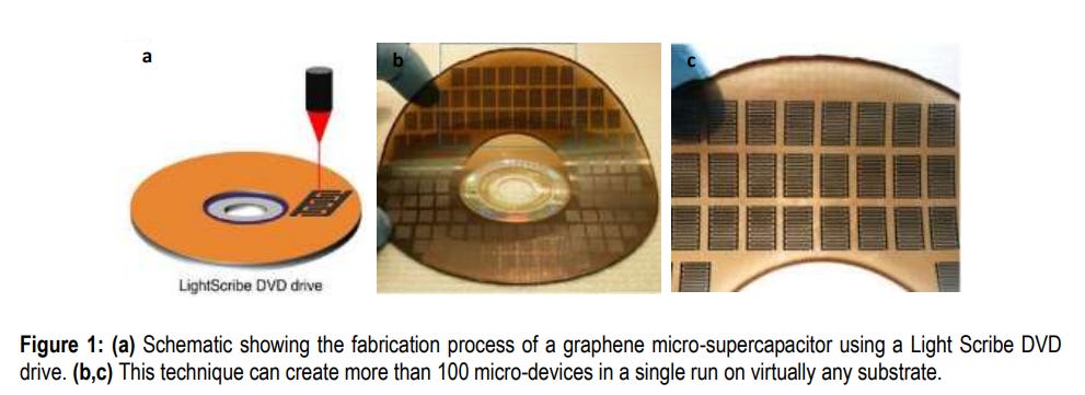
Abstract: Graphene is the ultimate two-dimensional material consisting of a single layer of sp2 hybridized carbon. A facile, inexpensive, solid-state method for generating, patterning and electronic tuning of laser converted graphene will be discussed. Briefly, graphite can be converted into graphene oxide (GO) sheets, which readily disperse in water, and can then be reduced by various methods. Due to its unique ability to be solution processed and patterned, GO can be laser reduced to graphene directly onto various substrates without masks, templates, post processing, or transfer techniques. This work paves the way for the fabrication of inexpensive electrochemical energy storage devices that combine the energy density of batteries and the power density of capacitors.
The summary of the second day will be published soon.
Don't hesitate to subscribe if you haven't already done so.
Regards and take care.


