GrapheneforUS – Day 2 (Summary)
The GrapheneforUS2021 Online Conference taked place during the 23-24 February
I would like to present in this post a summary of the second and last day.
I hope that will be of interest. Currently, the situation in the world does not allow us to travel to organize events and we have to carry out these events online that so far are being kindly accepted by the scientific community.
GrapheneforUS 2021 online was a 2 days event that means to gather the key players of the Graphene Community and related sectors. This event was launched again following the success of the 2018, 2019 & 2020 in-person editions and the lack of meetings in the field in the US. Graphenefor US is now already an established event attracting global participants and sharing, exchanging, exploring new avenues of graphene-related scientific and commercial developments.
The speakers of the second day with their titles were:
Robert Wallace (The University of Texas at Dallas, USA) - An update on contact reactions with TMDs
Joan Marie Redwing (The Pennsylvania State University, USA) - Progress in epitaxial growth of wafer-scale TMD monolayers
Zhihong Chen (Purdue University, USA) - 2D Materials for Back-end-of-line Interconnect Application
Filippo Giubileo (CNR-SPIN Università di Salerno, Italy) - Transition metal dichalcogenide monolayers as gate controlled field emitters
Philip Kim (Harvard University, USA) - Josephson Junctions based on van der Waals heterostuctures
Kaustav Banerjee (University of California, USA) - Next-generation integrated electronics uniquely enabled by van der Waals materials and heterostructures
Folkert de Vries (ETH Zurich, Switzerland) - Gate-Defined Josephson Junctions in Magic-Angle Twisted Bilayer Graphene
Jim Schuck (Columbia University, USA) - Nonlinear twistoptics at symmetry-broken interfaces
Jia Li (Brown University, USA) - Tuning moirè flatband in magic-angle twisted bilayer graphene
Stephan Roche (ICREA/ICN2, Spain) - Topological Spin Transport in Quantum Materials and Entanglement
Pablo Piskunow (Catalan Institute of Nanoscience and Nanotechnology, Spain) - Hinge Spin Polarization in Magnetic Topological Insulators Revealed by Resistance Switch
Stephen Power (Trinity College Dublin, Ireland) - Manipulating valley currents in graphene nanostructures
Megan Steves (The Pennsylvania State University, USA) - Correlating nonlinear optical properties with atomic-level structure in 2D-polar metals
Andrea Tomadin (Università di Pisa, Italy) - Microscopic theory of plasmon-enabled resonant terahertz detection in bilayer graphene
Raúl Guerrero (Centro de Física de Materiales, Spain) - Rhombohedral Phase in Trilayer-graphene
Ado Jorio (Universidade Federal de Minas Gerais, Brazil) - Phonon localization in low-angle twisted bilayer graphene
Jerzy Sadowski (Brookhaven National Laboratory, USA) - Interlayer coupling effects in the 30deg-twisted bilayer graphene
Jamie Warner (University of Texas at Austin, USA) - Air Stable Noble Metal Dichalcogenide 2D layered Materials
Rodney Ruoff (UNIST/CMCM, South Korea) - F-diamane from AB-stacked graphene
Michael Fuhrer (Monash University, Australia) - 2D Topological Insulators for Low-Energy Electronics
I would like to highlight some of the talks on this first day.
Bio: Rodney S. Ruoff, UNIST Distinguished Professor (The Departments of Chemistry and Materials Science, and The School of Energy Science and Chemical Engineering), directs the Center for Multidimensional Carbon Materials (CMCM), an Institute for Basic Science Center (IBS Center) located at the Ulsan National Institute of Science and Technology (UNIST) campus. Prior to joining UNIST in 2014, he was the Cockrell Family Regents Endowed Chair Professor at the University of Texas at Austin from September, 2007. He earned his Ph.D. in Chemical Physics from the University of Illinois-Urbana in 1988, and was a Fulbright Fellow in 1988-89 at the Max Planck Institute für Strömungsforschung in Göttingen, Germany. He was at Northwestern University from January 2000 to August 2007, where he was the John Evans Professor of Nanoengineering and director of NU’s Biologically Inspired Materials Institute. He has authored or co-authored over 500 peer-reviewed publications related to chemistry, physics, materials science, mechanics, and biomedical science. Rod is a Fellow of the Materials Research Society, the American Physical Society, the American Association for the Advancement of Science, and the Royal Society of Chemistry. He is the recipient of the 2014 Turnbull Prize from the MRS, the 2016 SGL Skakel Award from the American Carbon Society, the James C. McGroddy Prize for New Materials from the American Physical Society in 2018, and has been named a “Citation Laureate” (Clarivate Analytics). For further background on some of his research see: http://en.wikipedia.org/wiki/Rodney_S._Ruoff . [If of interest: Google Citation H-index 161, I-10 Index 503, 41 publications cited > 1000 times and 10 > 5000 times. A ‘highly cited researcher’ in Chemistry, Physics, and Materials Science, since such statistics have been reported by Thomson Reuters (and more recently by Clarivate Analytics).]
Abstract: I describe our conversion of AB-stacked bilayer graphene to the fluorinated diamane product, F-diamane, that can be thought of as an ultrathin (“2-atom thick”) layer of diamond that has “every other” C atom on each of the top and bottom surfaces functionalized by F: C2F stoichiometry. Time permitting, I will also describe some other research of probable interest. Support from the Institute for Basic Science (IBS-R019-D1) is appreciated
Figure: HRTEM cross section images of AB-stacked bilayer graphene (top left) and after its fluorination: F-diamane
Bio: Robert M. Wallace received his B.S. in Physics and Applied Mathematics in 1982 at the University of Pittsburgh where he also earned his M.S. (1984) and Ph.D. (1988) in Physics. From 1988 to 1990, he was a postdoctoral research associate in the Department of Chemistry at the Pittsburgh Surface Science Center. In 1990, he joined Texas Instruments Central Research Laboratories as a Member of Technical Staff (MTS) in the Materials Characterization Branch of the Materials Science Laboratory, and was elected as a Senior MTS in 1996. He was then appointed in 1997 to manage the Advanced Technology branch in TI’s R&D which focused on advanced device concepts and the associated material integration issues. In 2003, he joined the faculty in the Erik Jonsson School of Engineering and Computer Science at the University of Texas at Dallas as Professor and holds the Erik Jonsson Distinguished Chair in the Department of Materials Science & Engineering. Research interests include the study of surfaces and interfaces, particularly with applications to electronic materials and the resultant devices fabricated from them. These most recently include the study of compound semiconductor systems including arsenides (e.g. InGaAs), nitrides (e.g. GaN), phosphides (e.g. InP), as well as antimondies (e.g. GaSb), and 2D materials such as graphene and transition metal dichalcogenides. He was named Fellow of the AVS in 2007 and an IEEE Fellow in 2009 for his contributions to the field of high-k dielectrics in integrated circuits.
Abstract: Transition metal dichalcogenides (TMDs) are promising for applications in various electronic and photonics devices. MoS2, as one of the most studied TMDs, demonstrates impressive subthreshold slope, Ion/Ioff ratio and mobilities. However, the contact resistance of the highest-performance metal contacts to MoS2 based devices is orders of magnitude higher than that required for state-of-the-art logic circuits. Recent studies have noted that the contact resistance can be impacted by the deposition ambient of the metal contacts. Various metal contact (Au, Ti, Ir, Cr, and Sc) on MoS2 have been studied to understand their interface chemistry and the origin of Fermi level pinning under different deposition ambients. But the interface chemistry of now popular Ni and Ag contacts on MoS2 has not been systematically reported. CVD MoS2 films tend to have more intensive defects than the MoS2 bulk crystal. This difference in defect density could potentially impact the interface chemistry of the metal contacts on MoS2 and thus probably lead to different device performance. We will present an update of our prior study of deposition ambient effectsincorporating recent results with Ag and Ni contacts. This work was supported in part by NEWLIMITS, a center in nCORE, a Semiconductor Research Corporation (SRC) program sponsored by NIST through award number 70NANB17H041.
Figure: Schematic representations of the interface chemistry formed between contact metals (Ni, and Ag) and MoS2 substrates (MoS2 bulk, and 2L-MoS2 film).
Bio: Full Professor at the Physics Department and Member of the Brazilian Academy of Sciences. PhD from the UFMG, Postdoctoral fellow at Massachusetts Institute of Technology - MIT / USA, Director of Technology and Information in INMETRO, and Visiting Professor at ETH Zurich. Coordinator of the Brazilian Network for Research and Instrumentation in Optical Nanospectroscopy and considered one of "The World’s Most Influential Scientific Minds", according to the Thomson Reuters.
Abstract: Superconductivity has been found in bilayer graphene at the magic angle. Below the magic angle, the bilayer graphene exhibits reconstruction, entering the strain soliton regime. Direct optical images of the crystal superlattice in reconstructed twisted bilayer graphene are reported here , generated by nano-Raman spectroscopy . The observation of the crystallographic structure with visible light is made possible due to lattice dynamics localization, the images resembling spectral variations caused by the presence of strain solitons and topological points. The results are rationalized by a nearly-free-phonon model and electronic calculations that highlight the relevance of solitons and topological points, particularly pronounced for structures with small twist angles.
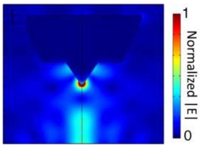
Figure: Nano-Raman field distribution generated in the tip-enhanced Raman spectroscopy (TERS) configuration
Bio: Zhihong Chen received her B.S. degree in physics from Fudan University in 1998, and her Ph.D. degree in physics from the University of Florida in 2003. After two years of postdoctoral research at IBM T.J. Watson research center, she became a research staff member in the Physical Science Department. Her research focused on design and fabrication of high performance carbon based devices and circuits. In 2008, she was appointed as the manager of the Carbon Technology Group at IBM, where she was in charge of evaluating the potential of carbon materials and the development of novel carbon based technologies for commercial applications. She joined the School of Electrical and Computer Engineering at Purdue University in 2010 as an Associate Professor, and has become a Full Professor since 2017. Her research interests focus on device and circuit designs for beyond-CMOS applications. She has become the Director of the SRC nCORE NEW LIMITS Center since 2018, and Associated Director of Research for Birck Nanotechnology Center in 2019. She is the Technical Program Chair for the 2020 Device Research Conference and General Chair for the 2021 DRC. She also serves as the Workshop Chair for the 2020 IEEE International Interconnect Technology Conference and Program Co-chair for the 2021 IITC.
Abstract: 2D materials have unique properties that can be utilized in designing next generation interconnects. For example, some 2D materials have been considered as alternative barrier/liner to replace conventional TaN/Ta bilayer, since these atomically thin materials are proven to be able to efficiently block Cu diffusion and their atomically thin body thickness can maximize Cu volume in ultra-scaled interconnects to achieve lower line resistance. In this talk, I will show that the diffusion barrier and liner properties of several 2D materials are investigated by various characterization methods. We observe that the lifetime of the dielectrics surrounding Cu electrodes can be significantly extended with the presence of the tested 2D barriers, providing strong evidence for promising alternative barrier/liner solutions.
Don't hesitate to subscribe if you haven't already done so.
Regards and take care.
The nanometer – 10 to the -9th meter- is a miniscule unit representing the world of nanoscience and nanotechnology, a field which is sometimes unknown but which has visible effects. With the aim of discovering what happens in the nanoworld and see what is being done in the fields of research and technology at a small scale, from April , the sixth edition of the Nanoscience and Nanotechnology Fest ival 10alamenos9 (www.10alamenos9.es) will take place.
The new edition of the festival, coordinated by the University of Barcelona, has more than a hundred activities, doubling the number of activities from last year’s edition. Fifty entities are taking part in the organization –universities and research institutes-, lots of them being reference entities in Iberoamerica in the field of nanotechnology.
The event is sponsored by BASF. Every year many (8) Iberoamerican countries organizes an outreach Festival with many activities, for example, this contest (https://icmab.es/concurs-de-nanorelats-organized-within-the-10alamenos9-festival). This event will take place in nine cities in Spain and other countries from April to May with activities aimed at the general public and schools, and it will have more than 5,000 participants.
The aim is to bring nanoscience and nanotechnology closer to people in a dynamic, fun and rigorous way and show people that nanotechnology is a reality, which is not seen but it is all over.
In Barcelona, there will be activities aimed at primary and secondary education schools –through the Nanoinventum/NAnoEduca project- apart from exhibitions, some with nanotechnology products and augmented reality, and seminars carried out by distinguished researchers, as well as workshops that are related to the several fields of nanoscience.
The Festival reaches its sixth edition from 2015. We made also some online activities possible such as the "Vermut de nanociència" with the main objective of bringing nanotechnologies to everybody in an understanding way and broadcasting it in streaming to make easier the participation and the debate. The talks started on April and ended on May. Last year we made 33 videos.
We are in touch
https://icn2.cat/en/outreach/education-program/10alamenos9
https://icmab.es/more-than-200-students-at-the-10alamenos9-nanoscience-and-nanotechnology-festival-at-uab-campus


